Five Bottlenecks Blocking 2D Semiconductors from the Fab
Silicon hit a wall. Now what?
Silicon transistors have been scaled below the 3 nm node, with channels just a few atoms thick. At this scale, quantum effects run wild. Tunneling leakage, short-channel effects, and thermal runaway all kick in simultaneously. Engineers spent two decades pushing silicon to its limits, and now physics says there is no road ahead.
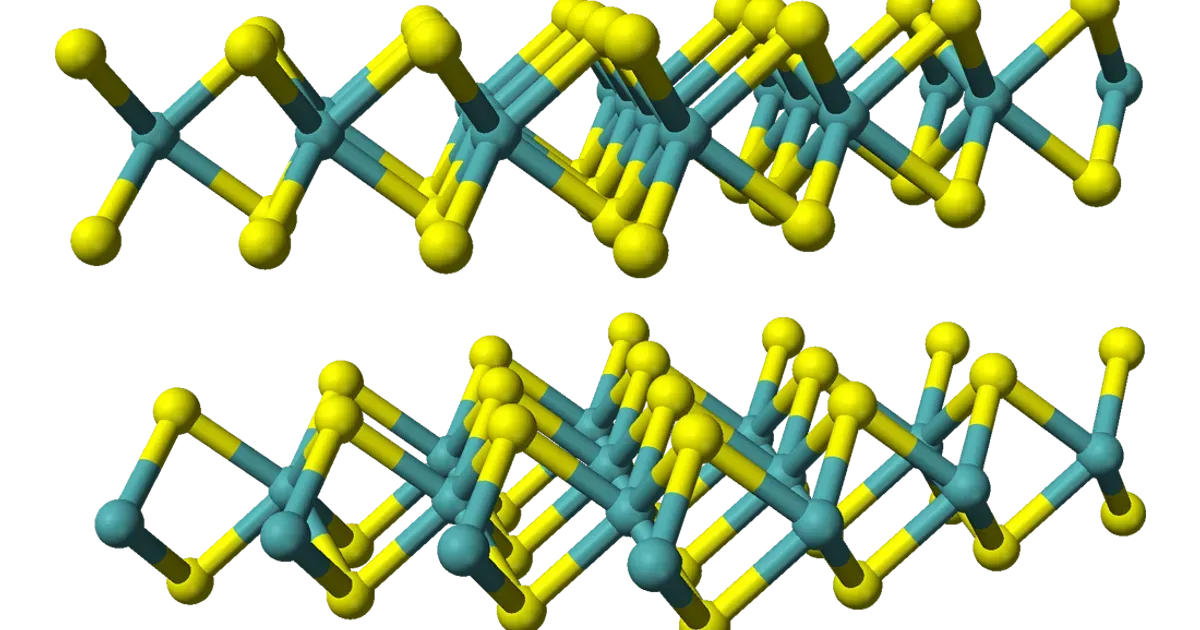
2D semiconductors stepped onto the stage at exactly this moment. Transition metal dichalcogenides (TMDs) like MoS₂ are atomically thin semiconductors by nature, with no dangling bonds and perfectly passivated surfaces. In theory, they can scale to ultra-short gate lengths without collapsing. Academic research exploded after 2011, and tens of thousands of papers have been published since.
But here is the catch. A single beautiful transistor demonstrated in the lab is worlds away from something a fab can mass-produce.
The 2D Semiconductor Family
Before diving into the bottlenecks, here is a quick tour of the material family. 2D semiconductors extend well beyond MoS₂.
MoS₂ (molybdenum disulfide) is the most-studied n-type 2D semiconductor, with a bandgap of about 1.8 eV (monolayer) and mobility exceeding 200 cm²/V·s under ideal conditions. WS₂ (tungsten disulfide) is structurally similar to MoS₂ but has stronger optical properties, making it suitable for optoelectronics. WSe₂ (tungsten diselenide) is one of the few p-type TMDs, a critical material for achieving complementary logic (CMOS). Black phosphorus has a tunable bandgap (0.3 to 2 eV) and high mobility, but oxidizes at a terrifying rate. hBN (hexagonal boron nitride) is technically an insulator, yet indispensable as the “ideal substrate” and dielectric layer for 2D materials.
They share a common trait. All are layered materials held together by van der Waals forces, which can be peeled apart one layer at a time using mechanical exfoliation. Perfect crystals without needing to be grown. Just peel them from a bulk crystal.
But what you peel off is only micrometers in size. For mass production, you need to “grow” these films on large-area substrates using chemical vapor deposition (CVD) and similar methods. That is where the first bottleneck begins.
Bottleneck 1: Contact Resistance
For any semiconductor to become a working transistor, metal electrodes must be placed at both ends to let current flow in and out. In the silicon world, this problem was solved decades ago. Ohmic contacts between metal and silicon can be made with extremely low resistance.
But when metal meets a 2D semiconductor, the situation is completely different.
The root cause is Fermi level pinning. When metal is deposited onto a 2D material, the metal’s electron wavefunctions penetrate into the semiconductor, creating so-called metal-induced gap states (MIGS) at the interface. These gap states pin the Fermi level at a fixed position within the bandgap, making it nearly impossible for engineers to tune the contact barrier height by simply choosing different metals.
The result: contact resistance stays stubbornly high no matter what metal you use. The best n-type contact resistance for MoS₂ is still in the tens to hundreds of Ω·μm range, while the industry target is below 10 Ω·μm. Still an order of magnitude away.
Several approaches are being explored. One uses semimetals like antimony (Sb) or bismuth (Bi) as contact materials, exploiting their ultra-low density of states to suppress MIGS. A 2025 Nature Electronics paper demonstrated crystalline antimony contacts achieving 98 Ω·μm at a contact length of 18 nm, the state of the art. Another approach is van der Waals contacts, where metal films are pre-fabricated and transferred onto the 2D material to avoid deposition-induced damage. A third is edge contacts, which touch only the side of the 2D material to minimize the interface area.
But p-type contacts lag far behind n-type. WSe₂ p-type contact resistance is still in the hundreds to thousands of Ω·μm range, the single biggest obstacle to building a 2D CMOS inverter.
Bottleneck 2: Large-Area Growth
In the lab, 2D semiconductors are typically made by mechanical exfoliation. Peeling a layer from a bulk crystal with adhesive tape and transferring it to a substrate. The material quality is excellent, but each flake is only micrometers to millimeters in size, with irregular shapes and random placement. Completely useless for mass production.
The only viable path to scale is CVD (chemical vapor deposition). Precursor powders (typically metal oxides) and chalcogen vapors (sulfur, selenium) are fed into a high-temperature furnace tube, where they react and deposit a 2D thin film on the substrate surface.
Sounds straightforward. But CVD growth of 2D semiconductors faces three core challenges.
The first is nucleation control. Nucleation sites on the substrate are randomly distributed. Too high a nucleation density produces many small grains that stitch together into a polycrystalline film with defective grain boundaries. Too low, and the grains never connect, leaving a discontinuous film. Achieving uniform nucleation density across an entire 6-inch or 8-inch wafer requires precise control of precursor concentration, temperature field, and gas flow field, three parameters that are coupled to each other, so adjusting one inevitably affects the other two.
The second is defect density. CVD-grown MoS₂ typically has a defect density on the order of 10¹² to 10¹³ cm⁻², two to three orders of magnitude higher than mechanically exfoliated samples. These defects (primarily sulfur vacancies) act as scattering centers, crushing mobility from the theoretical hundreds down to just 10 to 50 cm²/V·s. Worse, defects cause unstable carrier concentrations, making transistors at different positions on the same wafer behave very differently.
The third is phase control. TMDs exist in different crystal phases. MoS₂’s 2H phase is semiconducting, while its 1T phase is metallic. If temperature or precursor ratios drift during CVD, metallic 1T regions can appear in the film, directly shorting out the transistor channel. Maintaining pure 2H phase over large areas demands an extremely tight process window.
Bottleneck 3: Material Stability
2D materials are only one atom thick, meaning every single atom is exposed to the environment. This is fundamentally different from silicon. Once a native oxide layer forms on silicon, the surface is passivated. 2D materials have no such natural shield.
MoS₂ is relatively stable in air, but prolonged exposure still leads to adsorption of water molecules and oxygen, causing carrier concentration drift and mobility degradation. More serious is organic residue from the CVD process. Polymer materials like PMMA used during transfer and fabrication steps stick to the 2D material surface, degrading contact quality and altering the electronic band structure.
Black phosphorus is far worse. It begins oxidizing within minutes of air exposure, with phosphoric acid droplets forming on the surface. Unless the entire process is carried out in an inert atmosphere, or the material is fully encapsulated with hBN, practical applications are nearly impossible.
Long-term reliability is also a hidden concern for industrialization. Silicon devices have decades of accumulated reliability data, and failure rate curves are thoroughly understood. The longest reliability data for 2D semiconductor devices spans only a few years, a massive gap compared to the 10 to 20 year lifetime validation required for automotive or industrial-grade applications.
Bottleneck 4: Doping Control
Semiconductors derive much of their usefulness from doping. Introducing specific impurities to control whether a material is n-type or p-type, enabling p-n junctions and CMOS complementary logic gates.
Silicon doping technology has been refined over half a century. Ion implantation plus thermal annealing can precisely control dopant concentration and depth. But doping 2D semiconductors is an entirely different story.
The problem is dimensional constraint. 2D materials are only one atom thick. Conventional ion implantation would blast the crystal lattice apart. You simply cannot implant impurities into a single-atom-layer material without destroying its structure.
Current alternatives fall into three categories. The first is substitutional doping, where Nb (niobium) or V (vanadium) atoms are mixed directly into the CVD precursors, replacing Mo atoms to achieve p-type doping. Recent 2025 progress shows Nb-doped WSe₂ achieving hole mobility of 48 cm²/V·s with an on/off ratio of 10⁸. But concentration control remains coarse, and doping uniformity over large areas is still poor.
The second is surface charge transfer doping, where organic molecules (like BV²⁺ for n-type or Magic Blue for p-type) adsorb onto the 2D material surface to inject carriers. This method does not damage the lattice, but stability is terrible. Organic molecules easily desorb or degrade in air, causing device characteristics to drift over time.
The third is remote doping, where a dielectric layer separates the dopant source from the 2D material, using electrostatic induction to modulate carrier concentration. This approach has better stability, but doping efficiency is limited by the dielectric layer’s thickness and dielectric constant.
Overall, no single doping method for 2D semiconductors currently achieves precise control, lattice preservation, and long-term stability simultaneously. This is the single largest technical bottleneck to achieving 2D CMOS.
Bottleneck 5: Silicon Process Integration
Even if all four preceding bottlenecks are solved, one ultimate question remains. How do you put 2D semiconductors into an existing silicon fab?
The global semiconductor industry has accumulated tens of billions of dollars in equipment investment on silicon-based CMOS processes. Any new material that requires building a factory from scratch is economically unacceptable. For 2D semiconductors to truly industrialize, they must be manufacturable on existing 300 mm wafer production lines.
This imposes several hard constraints. First, growth temperature must stay below 400°C. 2D semiconductors are typically integrated at the back-end-of-line (BEOL), after metal interconnect layers are already in place. Temperatures above 400°C damage the underlying copper wiring and low-κ dielectrics. Current CVD growth of MoS₂ typically requires 700 to 1000°C, far exceeding this limit. Low-temperature CVD and atomic layer deposition (ALD) methods are under development, but quality still lags.
Second, transfer and alignment precision. If 2D materials are grown elsewhere and transferred to silicon wafers, the transfer process must achieve nanometer-level alignment accuracy to precisely match the underlying circuit patterns. Current transfer technology is far from meeting this requirement.
Third, dielectric layer compatibility. 2D transistors need high-κ gate dielectrics for good gate control. But high-κ materials like HfO₂ are typically grown by ALD, whose precursors struggle to nucleate uniformly on the inert surfaces of 2D materials, because there are no dangling bonds to provide reaction sites. This leads to non-uniform dielectrics, pinholes, and poor reliability.
Intel, TSMC, and Samsung have all invested in 2D semiconductor process integration research, but all remain at the proof-of-concept stage, at least 5 to 10 years away from volume manufacturing integration.
Prioritizing the Five Bottlenecks
If you had to rank them, contact resistance and doping control are the two bottlenecks the academic community agrees are most urgent. Without low-resistance contacts, transistor performance cannot improve. Without reliable doping, CMOS complementary logic cannot be built, and power consumption cannot come down.
Large-area growth and silicon process integration are the core industrialization barriers. They determine whether 2D semiconductors can move from papers to products. Material stability, while less “glamorous,” is the foundation of long-term reliability. Automotive and industrial applications cannot skip this step.
The good news is that progress is accelerating. The crystalline antimony Ohmic contacts reported in 2025 Nature Electronics, the precise p/n-type doping demonstrated in 2024 Nature Communications, and the centimeter-scale uniform WSe₂ film synthesis all show that these bottlenecks are being progressively dismantled.
2D semiconductors will not replace silicon tomorrow. But they are walking a path similar to SiC and GaN, from sporadic lab breakthroughs to repetitive engineering iterations, eventually finding a foothold in a specific application. The only difference is how long that road will take.
Related Posts
The Materials Science of Lithium-Ion Battery Recycling: Mining the Urban Mine
Battery recycling is not optional — 500,000 tons of Li-ion batteries will retire by 2025. But pyrometallurgy, hydrometallurgy, and direct regeneration each face different materials challenges.
The Materials Race in Carbon Capture: Amines, MOFs, and Zeolites
Carbon capture has been talked about for decades. The bottleneck is not engineering — it is materials chemistry.
The Real Bottleneck in Fusion Energy Isn't Plasma — It's Materials
Fusion reactors need materials that can withstand 150 million degrees and constant neutron bombardment. No known material can do this for long.