Perovskite Solar Cells: The Material Engineering Behind Record Efficiencies
Perovskite solar cells are the most closely watched new material system in photovoltaics since the silicon era. First reported at 3.8% efficiency in 2009, laboratory cells now exceed 26% as of 2024. That pace dwarfs crystalline silicon, which needed three decades to climb from 4% to 25%. Yet efficiency alone does not make a commercially viable technology. Two fundamental problems block the path from lab to factory floor: instability, and lead.
The Efficiency Trajectory
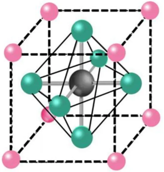
Perovskite refers not to a single mineral but to a family of materials sharing the ABX₃ crystal structure. In photovoltaic applications, the A site is typically an organic cation (methylammonium MA⁺ or formamidinium FA⁺), the B site is lead or tin, and the X site is a halide ion (iodine, bromine, or chlorine). This arrangement yields several decisive advantages over silicon.
The first is absorption coefficient. A perovskite film roughly 500 nm thick absorbs most incident sunlight. Crystalline silicon needs 100–200 µm — a factor of 200 to 400 times more material. This opens the door to lightweight, flexible, and semitransparent devices.
The second is carrier diffusion length. Photogenerated electrons and holes in perovskite can travel over a micron before recombining, long enough to reach the electrodes efficiently. Combined with defect tolerance — the material remains functional even with a high density of crystal defects, unlike conventional semiconductors — this makes it possible to fabricate high-efficiency cells using solution processing at low temperatures, without expensive epitaxial equipment.
Why Perovskite Degrades
Three degradation mechanisms act simultaneously, and they are intrinsic to the material.
Moisture sensitivity is the most straightforward. The organic cations are hygroscopic. Water molecules penetrate the crystal lattice, form hydrated intermediates, and trigger irreversible decomposition. A cell fabricated inside a glove box will show measurable efficiency loss after a few days of exposure to ambient humidity above 50%.
Photo-oxidation is harder to prevent. Illumination creates trap states that, in the presence of oxygen, catalyze the decomposition of the organic component. Encapsulation slows this process but cannot eliminate it entirely.
Ion migration is the most fundamental limitation. Halide ions and organic cations drift under the built-in electric field of the operating cell. This produces hysteresis in current-voltage curves, shifts the band structure over time, and eventually degrades performance. The activation energy for ion migration in typical perovskites is 0.1–0.6 eV, low enough that migration occurs at room temperature. Encapsulation does not stop it.
Current mitigation strategies include A-site doping (partial substitution of organic cations with cesium or rubidium), 2D/3D heterostructures, and interfacial passivation layers. These have pushed T₈₀ lifetimes (time to 80% of initial efficiency) from hours to thousands of hours in laboratory tests. Still, the gap to the silicon industry standard of 25+ years remains wide.
The Lead Problem
Every perovskite composition that holds a record efficiency contains lead. Lead is not incidental — it provides the electronic configuration that yields the optimal band gap and defect profile. No replacement has come close.
Tin-based perovskites (such as CsSnI₃) have a more ideal band gap on paper, but Sn²⁺ oxidizes readily to Sn⁴⁺ in air, destroying device performance within minutes without rigorous encapsulation. Antimony-based alternatives are more stable but lag far behind in efficiency, currently around 4%. No lead-free perovskite has exceeded 15%.
The debate is partly practical. Encapsulated lead perovskite modules are unlikely to leach lead during normal operation. But the environmental risk of millions of modules entering the waste stream or burning in wildfires at end of life remains poorly characterized at scale.
Silicon-Perovskite Tandems
Tandem cells are the application closest to commercialization. The principle is straightforward: perovskite has a wider band gap (1.5–1.7 eV) than silicon (1.1 eV). Stack them optically in series — the perovskite top cell absorbs high-energy photons, the silicon bottom cell captures the low-energy ones that pass through — and each operates near its own optimal wavelength.
Laboratory tandem efficiencies crossed 33% in 2024, with Oxford PV reporting 33.9%. That already exceeds the Shockley-Queisser limit for a single-junction silicon cell (~29%), and the theoretical limit for a dual-junction tandem is close to 50%.
The manufacturing challenge is thermal budget. The perovskite top layer must be deposited without degrading the silicon bottom cell, which restricts annealing temperatures to below 200°C. The tunnel junction (the recombination layer between the two sub-cells) requires careful optical and electrical design to minimize parasitic absorption and series resistance.
Perovskite Tandems Beyond Silicon
While silicon-perovskite tandems dominate headlines, perovskite can also pair with other thin-film bottom cells. CIGS (copper indium gallium selenide) is a natural partner: its band gap is tunable from 1.0 to 1.7 eV by adjusting the Ga/(Ga+In) ratio, and it already exists as a commercial thin-film product from manufacturers such as Solar Frontier and Avancis. A perovskite/CIGS tandem with a 1.6 eV perovskite top cell and a 1.1 eV CIGS bottom cell can reach theoretical efficiencies comparable to perovskite/silicon — and it can be fabricated entirely on lightweight flexible substrates such as polyimide foil, opening applications in building-integrated photovoltaics and portable power.
Cadmium telluride (CdTe) is another industrial thin-film platform with a band gap of 1.45 eV — too wide to serve as an efficient single-junction cell but well-matched as a bottom cell under a wide-band-gap perovskite top layer of 1.8 eV or higher. First Solar’s acquisition of Evolar in 2023 explicitly targets this pairing. The challenge with CdTe bottom cells is that CdTe requires a high-temperature activation treatment (typically above 400°C) that must be completed before the perovskite layer is deposited, constraining process sequence.
Beyond dual junctions, triple-junction architectures have been demonstrated in the laboratory using perovskite/perovskite/silicon stacks, with the middle perovskite layer tuned to an intermediate band gap. These have exceeded 27% in early demonstrations but introduce additional tunnel junction complexity and optical loss.
Institute-Industry Collaboration Models
The path from perovskite discovery to commercial deployment has been unusually direct — driven by deliberate knowledge transfer from academic groups to spin-off companies, rather than by established silicon incumbents.
The canonical case is Oxford PV. Founded in 2010 as a spin-out from the University of Oxford laboratories of Professor Henry Snaith — who co-authored the seminal 2012 paper demonstrating solid-state perovskite solar cells — the company has raised over £100 million in venture funding and built a pilot factory in Brandenburg, Germany. The model was straightforward: the university retained foundational IP, the company licensed it, and the academic group continued advancing the science while the spin-out focused on the engineering.
In Asia, the collaboration model differs. UNIST (Ulsan National Institute of Science and Technology) in South Korea has produced many of the highest-efficiency perovskite cells through close partnership with Korean chemical conglomerates. The Chinese Academy of Sciences has multiple perovskite research groups, several of which have direct cooperative agreements with manufacturers — notably the Institute of Chemistry CAS partnership with UtmoLight and the ShanghaiTech University collaboration with GCL Photoelectron. In Japan, Sekisui Chemical and Panasonic are developing perovskite films for building-integrated applications, drawing on long-standing thin-film expertise from the LCD industry.
A distinctive feature of the perovskite ecosystem is that much of the foundational IP originated in publicly funded university laboratories, creating a relatively open pre-competitive environment — conferences such as the International Conference on Perovskite Solar Cells (ICPSC) routinely feature detailed process disclosures that would be unusual in the silicon sector. This openness has accelerated progress but raises questions about long-term defensibility for individual manufacturers.
Machine Learning in Composition Screening
The ABX₃ perovskite compositional space is combinatorially vast. With dozens of candidate A-site cations, several B-site metals, three halide ions, and their arbitrary mixtures, the number of distinct compositions runs into the millions — far beyond the capacity of experimental trial. Machine learning has become an indispensable screening tool.
The dominant approach is a supervised regression pipeline: train a model on ~500 experimentally characterized compositions to predict photovoltaic-relevant properties (band gap, stability proxy, carrier lifetime), then screen virtual compositions in silico. Random forest and gradient-boosted tree models — particularly XGBoost — are preferred over deep neural networks because they perform well on the small, noisy datasets typical of early-stage materials discovery and yield interpretable feature importance rankings.
Key predictors include Goldschmidt tolerance factor, octahedral factor, ionic radii of the A-site cation, and formation enthalpy of competing decomposition phases. Stability prediction has proven harder than band gap prediction — no purely computed descriptor reliably captures the combined effects of moisture, oxygen, and illumination. Recent work has turned to Bayesian optimization under active learning loops, where a probabilistic model proposes candidates, a few dozen are synthesized and tested, and the model updates its prior, iterating toward stable high-performance compositions with fewer than 200 total experiments.
Generative models have also begun to appear. In 2023, researchers at MIT trained a variational autoencoder on perovskite crystal structures and used the latent space to propose compositions not previously reported in the literature. Several were synthesized and yielded photovoltaic activity. This approach remains early-stage but points toward a future where the screening bottleneck shifts from experimental throughput — which can be parallelized — to the intellectual bottleneck of deciding what to try.
Encapsulation Materials in Detail
Encapsulation is the single largest reliability challenge for perovskite modules, and material selection must address three independent pathways: moisture ingress, volatile organic out-diffusion, and electrode corrosion from halide migration.
Atomic layer deposition (ALD) Al₂O₃ is the most intensively studied primary barrier. ALD Al₂O₃ films as thin as 20 nm can achieve water vapor transmission rates (WVTR) below 10⁻⁵ g/m²/day — sufficient to protect the perovskite for operational lifetimes measured in years, though not yet decades. The key advantage of ALD is conformality: the film coats every surface feature, including module edges and scribe lines, providing a hermetic seal that sputtered or evaporated barriers cannot match on textured surfaces. ALD Al₂O₃ also acts as an ion migration barrier, suppressing halide diffusion into metal electrodes.
Parylene-C is emerging as a complementary organic barrier. Deposited by chemical vapor deposition at room temperature, parylene forms a pinhole-free polymer film with a WVTR around 10⁻³ g/m²/day — insufficient alone but effective when paired with an ALD inorganic layer. Its real contribution is mechanical: perovskite films undergo thermal expansion mismatches with glass and metal layers during temperature cycling. Parylene’s flexibility absorbs strain that would otherwise crack a brittle inorganic barrier.
Edge seal requirements are disproportionately demanding. The bulk of the module face is protected by glass and barrier films, but moisture ingress through edge adhesive — typically polyisobutylene (PIB) — must achieve WVTR on the order of 10⁻⁶ g/m²/day (three orders below silicon-module requirements) because the perovskite layer is hygroscopic at trace humidity levels. Laser-assisted frit bonding (a glass-to-glass seal formed by localized laser heating) is being tested as an alternative to polymer edge seals, offering WVTR effectively below measurement thresholds.
Economics: Perovskite vs Silicon Capex
The capital intensity of photovoltaic manufacturing has driven industry consolidation toward a handful of terawatt-scale silicon producers. Perovskite manufacturing promises a fundamentally different cost structure.
A state-of-the-art crystalline silicon cell and module factory costs approximately $100–120 million per gigawatt of annual nameplate capacity. Roughly half of that is the cell line — wafer texturing, diffusion furnaces, PECVD, screen printing — and half is module assembly. The single largest equipment item is the diffusion furnace, and the single largest facility cost is the cleanroom, because wafer handling demands Class 1000 or better throughout.
Perovskite manufacturing eliminates the wafer entirely. The cell is a thin-film stack deposited on glass, with no requirement for high-temperature diffusion or epitaxial growth. Slot-die coating equipment is commodity hardware borrowed from the flexible packaging and printed electronics industries, costing roughly $1–3 million per coating line. A perovskite module factory of 1 GW capacity has been estimated — in analyses published by the U.S. Department of Energy and Fraunhofer ISE — at $30–50 million, roughly one-third to one-half the capex of an equivalent silicon line.
The largest cost item shifts from the cleanroom to the encapsulation line: ALD and lamination equipment, plus the glass and edge-seal materials themselves. Material cost per square meter for perovskite modules is projected at roughly $20–30, compared to $25–35 for silicon modules — not dramatically lower, because the glass superstrate, encapsulant, junction boxes, and frames are shared across both technologies.
Where perovskite gains its decisive cost edge is in energy payback time. A silicon module requires roughly 1–2 years to generate the energy consumed in its manufacture. Perovskite modules, fabricated at low temperature with minimal thermal budget, have an estimated energy payback time of 2–4 months. For utility-scale deployment measured in hundreds of gigawatts, that difference compounds into a meaningful sustainability advantage.
Defect Tolerance in Depth
Defect tolerance is arguably the most remarkable physical property of perovskite, and it deserves closer examination. In conventional semiconductors such as silicon or gallium arsenide, deep-level defects — those with energy levels near mid-gap — act as efficient non-radiative recombination centers. A single such defect can kill the minority carrier lifetime over a large volume, which is why silicon solar cells require high-purity wafers grown via Czochralski or float-zone methods.
Perovskite sidesteps this constraint through its electronic structure. The valence band maximum and conduction band minimum in lead-halide perovskites are formed primarily by anti-bonding orbitals. When a vacancy or interstitial defect forms, the resulting defect states tend to fall within the band or near the band edge rather than deep in the gap. This “self-passivation” effect means that even a polycrystalline film with a high density of grain boundaries and point defects can maintain long carrier lifetimes and high photoluminescence quantum yields.
This property is what makes solution processing viable. Without defect tolerance, a spin-coated or slot-die coated film would contain too many recombination centers to function as a solar cell. Researchers are still working to understand this mechanism at the atomic level through ab initio calculations and advanced characterization techniques such as deep-level transient spectroscopy (DLTS) and thermally stimulated current (TSC) measurements.
Encapsulation and Reliability Testing
Encapsulation requirements for perovskite modules are significantly more demanding than those for crystalline silicon. Silicon modules need only protect against moisture ingress and mechanical stress. Perovskite modules must additionally block the out-diffusion of volatile organic species, prevent electrode corrosion from halide migration, and maintain optical clarity over decades.
The current state-of-the-art encapsulation strategy uses a multi-layer barrier stack. A thin film of Al₂O₃ or SiOₓ deposited by atomic layer deposition (ALD) serves as the primary moisture and ion barrier, typically 10–50 nm thick. This is followed by a polymeric edge sealant and a glass cover plate. The edge seal must achieve extremely low water vapor transmission rates (WVTR), on the order of 10⁻⁶ g/m²/day — three orders of magnitude lower than what suffices for silicon modules.
Reliability testing protocols for perovskite are still under active development. The silicon industry relies on IEC 61215, which includes damp heat (85°C / 85% relative humidity), thermal cycling, and UV preconditioning. Perovskite modules fail these tests in ways that silicon does not — combined light and humidity stress causes degradation that neither factor alone would produce. The International Summit on Perovskite Photovoltaic Stability (ISOS-PV) has proposed a dedicated set of protocols that include light-soaking at controlled temperature and humidity, maximum-power-point tracking during aging, and preconditioning steps that account for ion migration and burn-in effects. A consensus test standard is expected within the next few years and will be critical for bankability assessments by project financiers.
Manufacturing: Scalable Deposition Methods
Transferring perovskite cells from the spin-coater in a glove box to an industrial production line is a non-trivial engineering problem. Spin coating works well for small-area laboratory cells (typically 0.1 cm²) but is inherently wasteful and cannot scale to module-sized substrates. Two deposition methods have emerged as the leading candidates for mass production.
Slot-die coating is a solution-based method in which the perovskite precursor ink is extruded through a narrow slit onto a moving substrate. It is compatible with roll-to-roll processing on flexible substrates and can achieve coating speeds of several meters per minute. The challenges lie in ink formulation — the solvent system must evaporate at a controlled rate to produce uniform, pinhole-free films — and in managing the complex crystallization dynamics of perovskite. Additives such as dimethyl sulfoxide (DMSO) form intermediate phases that delay crystallization until the film is fully deposited; controlled annealing then drives the conversion to the final perovskite phase.
Thermal evaporation is a vacuum-based alternative that deposits the perovskite layer by layer from solid sources. It offers superior film uniformity and thickness control, which is critical for tandem cells where the perovskite layer must be optically tuned. The trade-off is higher capital equipment cost and lower throughput compared to slot-die coating. Oxford PV uses thermal evaporation for its tandem cells, while Chinese manufacturers such as UtmoLight favor solution processing for lower cost. Hybrid approaches also exist, where organic components are evaporated while the inorganic framework is deposited from solution, aiming to combine the advantages of both methods.
Tandem Architecture: Two-Terminal vs Four-Terminal
Tandem cells come in two fundamentally different configurations, each with distinct trade-offs.
Two-terminal (2T) monolithic tandems connect the perovskite top cell and silicon bottom cell electrically in series, with a tunnel junction between them. The two sub-cells share a single electrical circuit, so the currents must be matched — an effect known as current matching. If the top cell generates more current than the bottom cell, the excess is lost. This imposes tight tolerances on the perovskite band gap and layer thickness. The advantage of the 2T design is that it requires only one external electrical connection and can be manufactured with relatively minor modifications to existing silicon cell production lines. Oxford PV’s 33.9% record used a 2T monolithic architecture.
Four-terminal (4T) mechanical stacks are optically coupled but electrically independent. Each sub-cell has its own pair of electrodes and operates at its own maximum power point. This eliminates the current-matching constraint and relaxes the band gap requirements. The 4T design is easier to fabricate initially, because the perovskite top cell can be made on a separate superstrate and laminated onto a finished silicon cell. The penalty is added complexity in wiring and inverters, plus parasitic absorption in the transparent electrode and intermediate layer. For utility-scale deployment, balance-of-system costs tend to favor 2T designs, but 4T offers a faster path to market for early production.
Industry Roadmaps and Market Projections
The International Technology Roadmap for Photovoltaic (ITRPV) has included perovskite/silicon tandem cells in its projections since 2022. The 2024 edition forecasts that tandem cells will capture approximately 5% of the global photovoltaic market by 2028 and exceed 15% by 2032, driven by the need to push module efficiency beyond the practical ceiling of single-junction silicon.
Company-level progress supports this trajectory. Oxford PV began pilot production at its Brandenburg factory in Germany in 2024 with an initial capacity of 100 MW per year and has announced plans to scale to 1 GW by 2028. UtmoLight, based in Wuxi, China, operates a 150 MW pilot line producing single-junction perovskite modules and has reported module efficiencies above 18% on an area of 30 × 30 cm². First Solar, the largest thin-film manufacturer in the United States, acquired the perovskite startup Evolar in 2023 and is integrating the technology into its cadmium telluride platform, targeting tandem module efficiencies above 25%. LONGi Green Energy, the world’s largest silicon solar cell manufacturer, has set an internal tandem cell efficiency record of over 33% on a small-area lab cell.
Notably, China has emerged as the largest source of perovskite patents globally, accounting for over 40% of filings, and the government has included perovskite in its latest Five-Year Plan for renewable energy technology development. Whether the technology can achieve the reliability and manufacturing yield needed for terawatt-scale deployment remains the open question — but the pace of investment suggests the industry is treating it as a matter of when, not if.
Outlook
Perovskite solar cells have proven themselves on efficiency. Silicon-perovskite tandems already exceed 33% in the laboratory, surpassing the practical ceiling of single-junction silicon. The open questions — stability at 25-year timescales, lead toxicity at end-of-life, and manufacturing yield at gigawatt scale — are engineering problems with active, well-funded pathways toward resolution. The next decade will determine whether the technology reaches terawatt scale. The pace of investment, patent activity, and academic-industry knowledge transfer suggests the industry is treating it as a matter of when, not if.
Related Posts
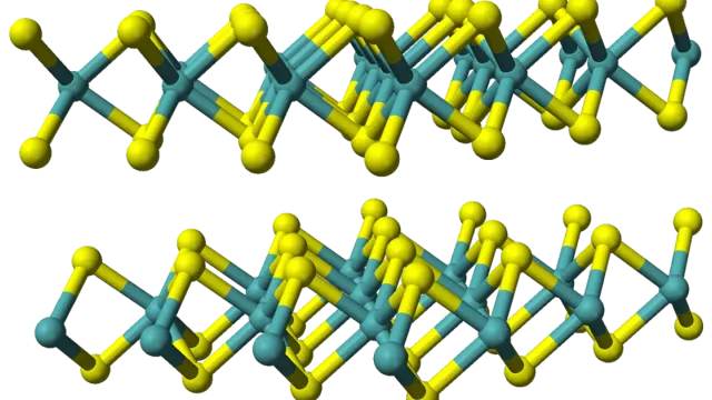
Five Bottlenecks Blocking 2D Semiconductors from the Fab
MoS₂, WS₂ and other 2D semiconductors promise to extend Moore's Law, but at least five industrialization bottlenecks stand between a lab-scale flake and a wafer-scale product.
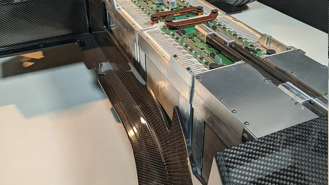
The Materials Science of Lithium-Ion Battery Recycling: Mining the Urban Mine
Battery recycling is not optional — 500,000 tons of Li-ion batteries will retire by 2025. But pyrometallurgy, hydrometallurgy, and direct regeneration each face different materials challenges.
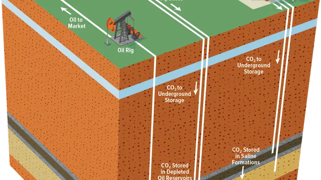
The Materials Race in Carbon Capture: Amines, MOFs, and Zeolites
Carbon capture has been talked about for decades. The bottleneck is not engineering — it is materials chemistry.